The Engineering Cleanroom Facility consists of an ISO 7 (class 10,000) cleanroom equipped for microlithography, and a supporting process room facility. Capabilities include:
- Thin film, evaporation of metals including gold, silver, chrome, aluminium and zinc
- Wet etch facilities and expertise
- Wafer dicing
- Plasma cleaning and surface functionalisation
- Inert atmosphere curing and vacuum oven
- Lapping/polishing
- Ink jet printing (DIMATIX DMP-2850)
- Photolithography at 4” wafer scale down to 10 micron resolution
- Spin coating
- Direct writing photolithography with 1 mm write field
- Microscopy
- Atomic force microscopy
- Profilometry
- Ball and wedge bonding and micro riveting
- Contact angle measurements
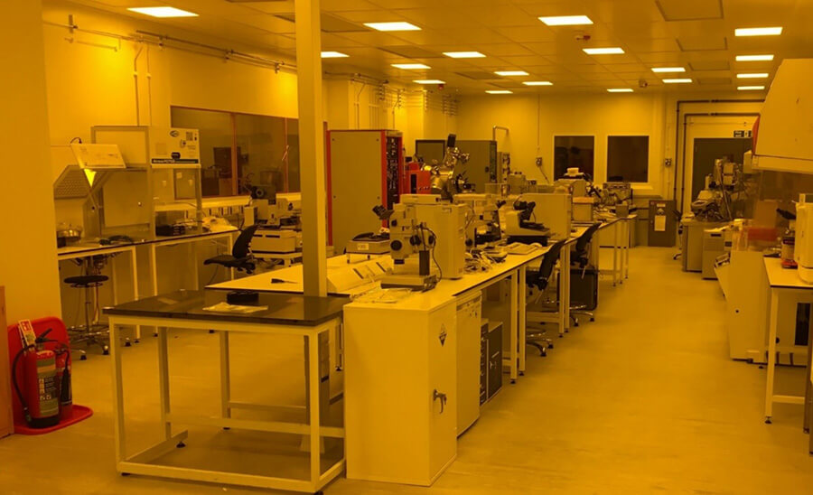 The EDT clean room