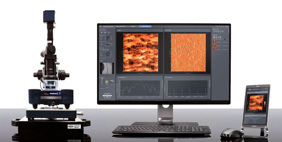
Bruker NanoWizard 4
The Bruker Nanowizard 4 is an Atomic Force microscope capable of producing very high-resolution scans in the order of a fraction of a nanometer. A mechanical probe utilises “PeakForce Tapping” to interact with the surface of the sample.
The AFM has applications in force measurement, 3D topographic imaging and nano-manipulation. For more information and specifications please consult the Bruker Nanowizard 4 brochure (pdf 3100 KB) .
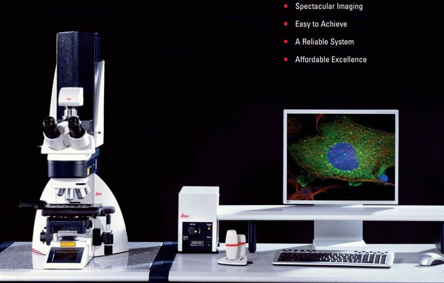
Leica Confocal TCS SPE
The Leica TCS SPE is a spectral confocal microscope which produces high resolution 3D images over the full spectral range. Optimal excitation is ensured by four solid state lasers from 488nm to 635nm.
The most common use of the microscope is to obtain clean 3-dimensional images using immunohistochemistry staining techniques. For more information and specifications please consult the Leica confocal TCS SPE brochure (pdf 6000 KB).
Bruker SkyScan 1172 Micro CT
The Skyscan 1172 is a desktop ex vivo micro-CT specimen scanner. The device works by obtaining multiple x-ray transmission images of an object from multiple angular views. Cross-sectional images of the object are then algorithmically constructed. The Skyscan creates a complete 3D representation of the internal microstructure and density from a selected horizontal region of the transmission image.
This allows in-depth quantitative data to be obtained on the 3D structure of samples such as soft tissues, bone, cartilage, composite materials, fuel cells, rocks and more. The process is non-destructive and requires no sample preparation or thin slicing, a single scan can image a sample’s complete internal 3D structure at high resolution. The maximum sample size can be 25mm in diameter for a standard scan and 50mm in diameter for a scan with camera offset.
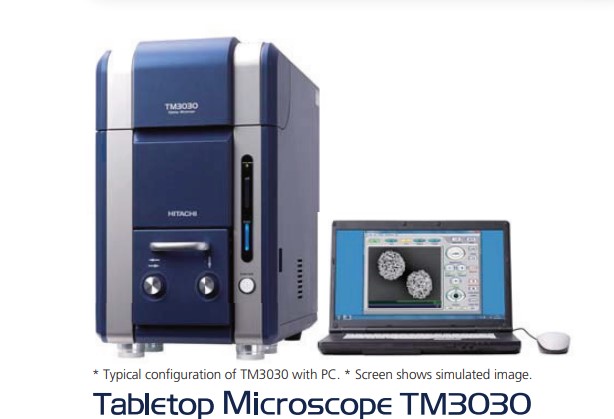
Hitachi TM3030 plus
The Hitachi TM3030 is a high-resolution scanning electron microscope. It can accommodate specimens up to 70mm in diameter and 50mm thick. It can be used to measure topographical features, to determine phase separation of metals and ceramics, to image non-conductive materials, to find weight and atomic percent composition down to 1% accuracy.
It can be used for magnification up to 30,000x. For more information and specifications about the Hitachi TM3030 brochure (pdf 9820 KB).
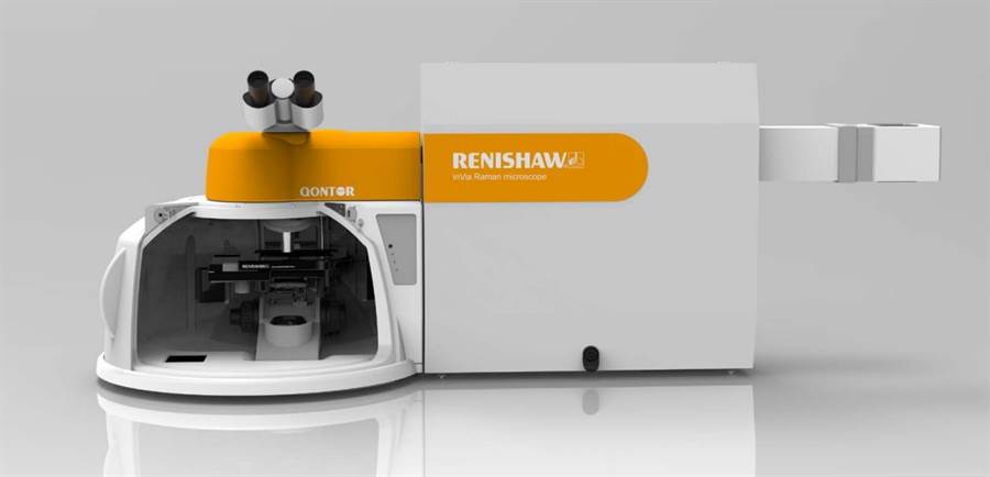
Renishaw InVia Raman Microscope
The Renishaw InVia Raman microscope yields high resolution Raman spectra of samples for determination of molecular compositions and bonding. The instrument is automated for ease of use and enables both point analysis and mapping.
The techniques that can be used with the device include phase identification and discrimination of mineral polymorphs, analysis of the effects of bonding, environment, and stress on a sample, and determination of crystallinity, crystal symmetry and orientation.
For more information and specifications please consult the Renishaw InVia Raman Microscope brochure (pdf 4000 KB)